


The race to achieve ever smaller production processes is far from over, as evidenced by IBM announcing the first chips. 2-nanometer manufacturing process. Invention, which is defined by the company as “disruptive” (which uses the English word Breakthrough), Is the result of IBM research, which comes four years after the first 5 nm chips were announced.
Small and efficient chips: IBM introduces 2nm manufacturing process
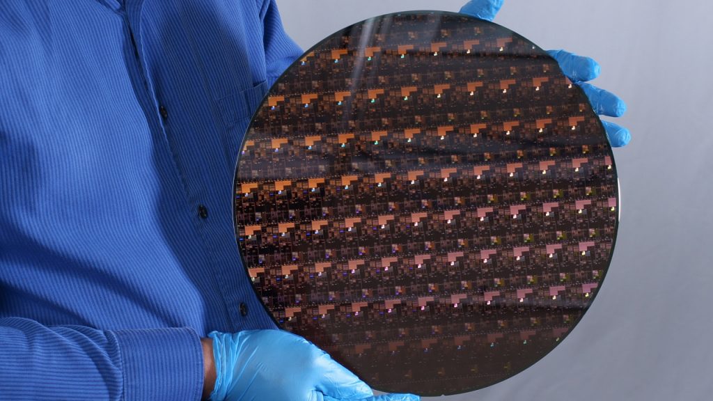
IBM today presented a significant improvement in the miniaturization of transistors, resulting in microchips using them. The company has further developed its technique Silicon nanosheets (Silicon nanosheet technology) Bringing it to the finish line 2 N.M.: It is the first company in the world to reach this milestone, beating Laurel in a size reduction race. This can be achieved by the Albany Nanotech Campus Research Center in Albany, New York, where IBM conducts research in collaboration with public and private companies.

IBM’s technique involves application Silicone sheets Two nanometers thick to create the structure of transistors instead of the use of traditional finfits. In this way, the company claims to have exceeded the limits imposed by this technology commonly used in semiconductor manufacturing today: the device you read this message on has a processor that uses Finfet technology, by all means.
IBM previously used this technique for its 5nm process and has now refined it. An interesting feature of the IBM approach is that for its 5nm production process, the same EUV lithographic process is used (Intense UV) 7 Nm is used today for the production process, so no further reduction is required. This is a very important detail as the lithographic process is always one of the obstacles in the production of small semiconductors. It is currently unknown whether even the 2 nm process can reuse the same lithography of a 7 nm process, but given the similarities with the 5 nm process we do not realize this possibility can be ruled out.
It will be produced in 2nm, compared to the 7nm processors used today 45% higher efficiency With the same consumption or one 75% reduction in energy used With the same performance. Simultaneously there is likely to be an increase in performance and lower overall consumption, which will lead to faster and longer battery life for the various electronic devices we use on a daily basis.
Thanks to this invention, IBM says you can enter 50 billion transistors The size of a fingernail in a microchip: To provide a measurement sequence, the AMD EPOC ROM processors produced at 7 nm have about 39.5 billion transistors, which have a surface area of about 1000 mm, while the Apple M1 that produces 5 nm has an area of approximately 119 mm. 16 billion transistors.
It is not known when this manufacturing process will be used for the production of large-scale microchips, but it will certainly take some time: what IBM announced today is the first step that will lead to the spread of technology in the future.
One step up, but there are obstacles to the road
This announcement moves the semiconductor world to a little more date to find out Alternative to silicon: Solvable problems were assumed with the approach of production dimensions as announced by IBM a few years ago, but with today’s announcement, it is no longer possible to derive an increase in efficiency from a reduction in the production process. And the alternative must be evaluated. Silicone-like semi-silicone is one of the most promising alternatives, but it is much cheaper and cheaper than silicon.

“Avid writer. Subtly charming alcohol fanatic. Total twitter junkie. Coffee enthusiast. Proud gamer. Web aficionado. Music advocate. Zombie lover. Reader.”


More Stories
Acrylic Nails for the Modern Professional: Balancing Style and Practicality
The Majestic Journey of the African Spurred Tortoise: A Guide to Care and Habitat
Choosing Between a Russian and a Greek Tortoise: What You Need to Know